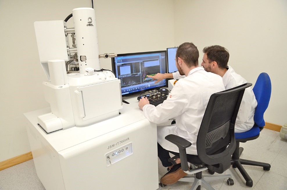
“This new resource will further increase TECNALIA’s ability to provide innovative solutions to boost the development of new materials”
Discover the characterisation of materials on a nanometric scale with TECNALIA’s high-resolution FE-SEM electron microscope
TECNALIA’s materialography laboratory has a new field emission scanning electron microscope (FE-SEM) that is especially suitable for surface characterisation in a wide variety of fields, from materials science to medicine and biology.
The FE-SEM is a state-of-the-art tool that allows imaging on a nanometric scale with unprecedented resolution.
- Its ability to perform semi-quantitative analysis at high speed makes it an indispensable tool for the characterisation of a wide variety of samples, including metallic, non-metallic and even heat-sensitive materials.
- This microscope has a high and low vacuum configuration, which facilitates the analysis of both conductive and non-conductive samples.
- It is also possible to work at low acceleration potentials which will allow the observation of heat-sensitive samples such as biological samples, membranes and lightweight composites.
The field emission scanning electron microscope (FE-SEM) analyses a wide range of materials
- Metals and alloys: steel, aluminium, copper, titanium, iron, nickel, among others.
- Ceramics and ceramic materials: metal oxides, advanced ceramics, refractory materials, glass.
- Polymers and composites: plastics, elastomers, fibre reinforced polymers, polymer matrix composites, resins.
- Semiconductor materials: silicon, germanium, gallium arsenide, gallium nitride, doped materials.
- Biological materials: cells, biological tissues, viruses, bacteria.
- Organic materials: organic compounds, synthetic materials, organic polymers.
- Heat-sensitive materials: materials that can be affected by high temperatures, such as thermoplastic polymers, thermosetting organic materials, among others.
- Nanostructured materials: nanoparticles, carbon nanotubes, nanocomposites, materials with dimensions on a nanometric scale.
Advantages of working with an FE-SEM
The main advantages of working with an FE-SEM include improved spatial resolution (with highly focused high- and low-energy electron beams), higher analytical speed and the possibility to conduct non-metallic and/or heat-sensitive sample analysis.
From identifying surface defects to studying the microstructure of materials, FE-SEM provides detailed insight that facilitates informed decision-making in product and process development.
With the new FE-SEM, TECNALIA has strengthened its commitment to providing customers with the most advanced tools to address the most complex challenges in materials research and development.

